Embibe Experts Solutions for Chapter: Semiconductor Devices, Exercise 2: Exercise-2
Embibe Experts Physics Solutions for Exercise - Embibe Experts Solutions for Chapter: Semiconductor Devices, Exercise 2: Exercise-2
Attempt the free practice questions on Chapter 35: Semiconductor Devices, Exercise 2: Exercise-2 with hints and solutions to strengthen your understanding. Beta Question Bank for Engineering: Physics solutions are prepared by Experienced Embibe Experts.
Questions from Embibe Experts Solutions for Chapter: Semiconductor Devices, Exercise 2: Exercise-2 with Hints & Solutions
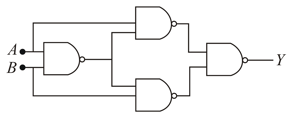
The truth table for the following combination of gates is:
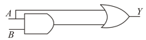
The combination of the gates shown represents:
Which of the following relations is valid for Boolean algebra:
In the following circuit, the output for all possible inputs and is expressed by the truth table:
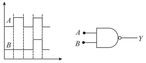
The real time variation of input signals and are as shown below. If the inputs are fed into gate, then select the output signal from the following:
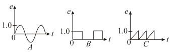
The time variations of signals are given as in and . Point out the statement from the following:
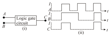
The following figure shows a logic gate circuit with two inputs and and output . The voltage waveforms of and are as shown in second figure given below:
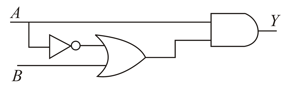
The logic circuit gate is:
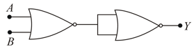
Select the outputs of the combination of gates shown below for inputs and respectively: