
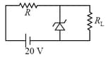
A Zener diode along with a series resistance is connected across a supply (as shown in the figure). If the maximum Zener current is , then the minimum value of will be _____ .
Important Questions on Electronic Devices Semiconductors
A modulating signal is a square wave, as shown in the figure.
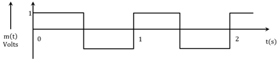
If the carrier wave is given as volts, the modulation index is:
Given below are two statements: one is labelled as Assertion A and the other is labelled as Reason R.
Assertion A: Photodiodes are preferably operated in reverse bias condition for light intensity measurement.
Reason R: The current in the forward bias is more than the current in the reverse bias for a junction diode.
In the light of the above statement, choose the correct answer from the options given below :
Match List I with List II
| LIST I | LIST II | ||
| A | AM Broadcast | I | |
| B | FM Broadcast | II | |
| C | Television | III | |
| D | Satellite Communication | IV |
Choose the correct answer from the options given below:
Given below are two statements : one is labelled as Assertion A and the other is labelled as Reason R
Assertion A: Photodiodes are used in forward bias usually for measuring the light intensity.
Reason R: For a junction diode, at applied voltage the current in the forward bias is more than the current in the reverse bias for where is the threshold voltage and is the breakdown voltage.
In the light of the above statements, choose the correct answer from the options given below
Statement I : When a Si sample is doped with Boron, it becomes P type and when doped by Arsenic it becomes N-type semi conductor such that P-type has excess holes and N-type has excess electrons.
Statement II : When such P-type and N-type semi-conductors, are fused to make a junction, a current will automatically flow which can be detected with an externally connected ammeter.
In the light of above statements, choose the most appropriate answer from the options given below.
Match List I with List II
| List I | List II | ||
| A | Troposphere | I | Approximate over Earth’s surface |
| B | E-Part of Stratosphere | II | Approximate over Earth’s surface |
| C | -Part of Thermosphere | III | Approximate over Earth’s surface |
| D | D-Part of Stratosphere | IV | Approximate over Earth’s surface |
Choose the correct answer from the options given below :


