Draw the symbol of an N-P-N transistor.
Important Questions on Semiconductor Devices
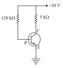
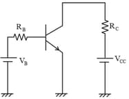
In the figure, given that supply can vary from to and The minimum base current and the input voltage at which the transistor will go to saturation, will be, respectively:
In the following circuit, the value of is and is Identify the correct statement:
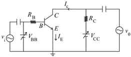
If is the emitter current, the base current and the collector current of a transistor, then which of the following statements are NOT TRUE?
(i)
(ii)
(iii)
(iv)
The transfer characteristic curve of a transistor, having input and output resistance and respectively, is shown in the figure. The voltage and power gain, are respectively:
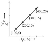
current gain will be (Round off to the Nearest Integer)
An n-p-n transistor has three leads A, B and C. Connecting B and C by moist fingers, A to the positive lead of an ammeter, and C to the negative lead of the ammeter, one finds large deflection. Then, A, B and C refer respectively to :
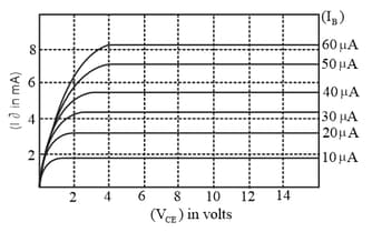
The output characteristics of a transistor is shown in the figure. When is and , then value of is