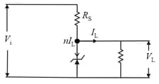
Explain zener breakdown.
Important Questions on Semiconductor Devices
Draw circuit diagram for a junction to obtain reverse bias characteristic curves. Explain the phenomenon of reverse breakdown for a junction in reverse bias state by following process-
Zener breakdown

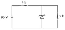
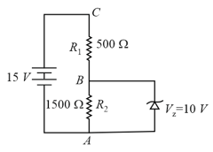
The current through the Zener is:
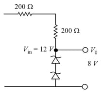
Two Zener diodes ( and ) having breakdown voltages of and respectively, are connected as shown in the circuit below. The output voltage variation with input voltage linearly increasing with time, is given by ()
What will be the current flowing through the resistor in the circuit shown, where the breakdown voltage of the Zener is

The Zener diode shown in the figure has negligible resistance and a knee current of . The minimum value of so that the voltage across it does not fall below is
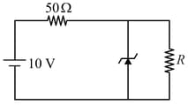
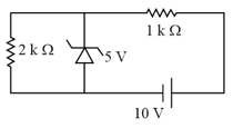
In the circuit shown, what will be the current through the zener?
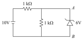
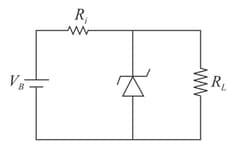
The zener diode has a . The current passing through the diode for the following circuit is___
In case of a p-n junction diode at high value of reverse bias, the current rises sharply. The value of reverse bias is known as
Avalanche breakdown is primarily dependent upon the phenomenon of:
Take the breakdown voltage of the zener diode used in the given circuit as . For the input voltage shown in the figure below, the time variation of the output voltage is: (Graphs drawn are schematic and not to the scale)

In which bias can a Zener diode be used as voltage regulator?
In connection with the circuit drawn below, the value of current flowing through resistor is______
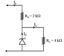
The value of the resistor, , needed in the DC voltage regulator circuit shown here, equals:
