
How do you find the operating point of a transistor?
Important Questions on Semiconductor Devices
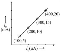
The transfer characteristic curve of a transistor, having input and output resistance and respectively, is shown in the figure. The voltage and power gain, are respectively:
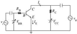
In the following common emitter circuit, and . If is negligible, then the base current is
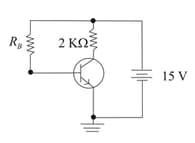
In the circuit shown, the value of of the transistor is . If the supplied base current is , what is the voltage at the terminal ?
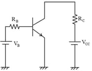
In the figure, given that supply can vary from to and The minimum base current and the input voltage at which the transistor will go to saturation, will be, respectively:
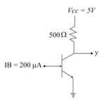
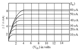
The output characteristics of a transistor is shown in the figure. When is and , then value of is
An n-p-n transistor has three leads A, B and C. Connecting B and C by moist fingers, A to the positive lead of an ammeter, and C to the negative lead of the ammeter, one finds large deflection. Then, A, B and C refer respectively to :


