
How does the depletion region of a junction diode get affected under reverse bias?
Important Questions on Electronic Devices
Why does the base region of a transistor is thin and lightly doped ?
The output of an unregulated dc power supply needs to be regulated. Name the device that can be used for this purpose and draw the relevant circuit diagram.
Two semiconductor materials and shown in Fig. are made by doping germanium crystal with indium and arsenic respectively. The two are joined end to end and connected to a battery as shown.
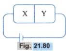
Sketch a - graph for this arrangement.
What do the terms ‘depletion region’ and ‘barrier potential' mean for a junction?
In a transistor, the doping level in the base is increased slightly. How will it affect
collector current and
In a transistor, doping level in base is increased slightly. How will it affect
base current.
What happens to the width of depletion layer of a junction when it is
(i) forward biased
What happens to the width of depletion layer of a junction when it is
(ii) reverse biased?


