
EASY
JEE Advanced
IMPORTANT
Earn 100
In forward bias, the width of potential barrier in a p-n junction diode
100% studentsanswered this correctly
Important Questions on Solids and Semiconductor Devices
EASY
JEE Advanced
IMPORTANT
The dominant mechanisms for motion of charge carriers in forward and reverse biased silicon junctions are,
EASY
JEE Advanced
IMPORTANT
In junction, avalanche current flows in circuit when biasing is,
EASY
JEE Advanced
IMPORTANT
When forward bias is applied to a junction, what happens to the potential barrier and the width of charge depleted region ?
MEDIUM
JEE Advanced
IMPORTANT
A potential barrier of exists across a junction. If the depletion region is wide, the intensity of the electric field in this region is,
EASY
JEE Advanced
IMPORTANT
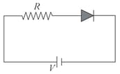
For the given circuit of junction diode, which of the following statement is correct?
EASY
JEE Advanced
IMPORTANT
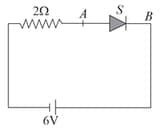
The diode shown in the circuit is a silicon diode. The potential difference between the points and will be,
EASY
JEE Advanced
IMPORTANT
A diode having potential difference across its junction, which does not depend on current, is connected in series with resistance of across source. If passes through resistance, then what is the voltage of the source?
EASY
JEE Advanced
IMPORTANT
Potential barrier developed in a junction diode opposes,


