
The conductivity of an intrinsic semiconductor depends on temperatures as , where is a constant. Find the temperature at which the conductivity of an intrinsic germanium semiconductor will be double of its value at . Assume that the gap for germanium is and remains constant as the temperature is increased.
Important Points to Remember in Chapter -1 - Semiconductors and Semiconductor Devices from H C Verma CONCEPTS OF PHYSICS [VOLUME 2] Solutions
1. Energy Bands in Solids:
(i) Valence band: The energy band formed by a series of energy levels containing valence electrons is known as valence band.
(ii) Conduction band: The higher energy level band is called the conduction band.
(iii) Conduction band: The higher energy level band is called the conduction band.
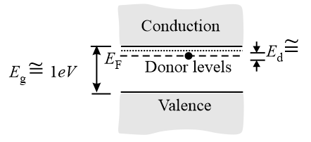
(iv) Forbidden energy gap : Energy gap between the conduction band and valence band
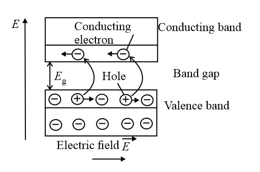
Note: No free electron is present in the forbidden energy gap.
(v) Fermi energy level: The highest energy level which can be occupied by an electron in valence band at is called fermi level.

2. Semiconductors:
(i) Holes in Semiconductors: When an electron is removed from a covalent bond, it leaves a vacancy behind. An electron from a neighbouring atom can move into this vacancy, leaving the neighbour with a vacancy. In this way, the vacancy formed is called hole and can travel through the material and serves as an additional current carrier. Hole acts as a virtual charge, although there is no physical charge on it. The mobility of hole is less than the electron.
(ii) Conductivity of semiconductor: where, mobility of electron and mobility of holes
3. Types of Semiconductor:
| Intrinsic semiconductor | P-type semiconductor | N-type semiconductor |
| Semiconductor in its pure form | Semiconductor after doping with trivalent impurity | Semiconductors offer doping with pentavalent impurity |
| Electrically neutral | Electrically neutral | Electrically neutral |
| Holes & electrons are equal | Holes are majority carriers | Electrons are majority carries |
| Net current, but | , but | , but |
| Acceptor impurity | Donor impurity | |
| FEL lies at the middle between VB and CB. | FEL lies just above VB. | FEL lies just below CB. |
| At , it acts as an insulator. | It shows conductivity at . | It shows conductivity at . |
| With increase in temperature, doesn’t change | With increase in temperature increases, but | With increase in temperature, decreases, but |
4. P-N Junction Diode:
When a -type semiconductor is suitably joined to an -type semiconductor, the resulting arrangement is called junction or junction diode.
(i) Depletion region: On account of the difference in concentration of charge carriers in the two sections of junction, the electrons from -region diffuse through the junction into -region and the hole from region diffuse into region.
Width of the depletion layer
(ii) Potential barrier: The potential difference created across the junction due to the diffusion of electrons and holes is called as potential barrier.
For , and for silicon,
5. Biasing of a P-N junction diode:
| Forward bias | Reverse bias |
| 1) -region is connected higher potential and n-region is connected to lower potential | 1) -region is connected to lower potential and n-region is connected to higher potential |
| 2) | 2) |
| 3) Width of depletion layer decreases. | 3) Width of the depletion layer increases. |
| 4) Forward resistance of an ideal diode is zero. | 4) Reverse resistance of an ideal diode is infinity. |
| 5) Potential barrier decreases. | 5) Potential barrier increases. |
6. Reverse Breakdown:
If the reverse-biased is too high, then a breakdown of junction diode occurs. It occurs in two ways,
(i) Zener breakdown: Breaking of covalent bonds due to a strong electric field in the reverse direction.
(ii) Avalanche breakdown: Breaking of covalent bonds due to collision between high-speed electron and valence electron.
Both Zener and avalanche breakdown occur simultaneously.
7. Zener Diode:
It is a heavily doped diode that works as a voltage regulator in reverse bias. It allows different values of current at reverse breakdown voltage. Zener voltage depends on the material of the semiconductor and doping concentration.
8. Zener Diode as Voltage Regulator:
If by keeping constant, then and but constant
If by keeping constant, then constant, and but constant
9. Half wave rectifier:
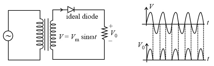
When the junction diode rectifies half of the wave, it is called a half-wave rectifier.
(i) Average output in one cycle: and ( forward-biased resistance)
(ii) RMS output:
(iii) The ratio of the effective alternating component of the output voltage or current to the component is known as the ripple factor.
(iv) Peak inverse voltage : The maximum reverse-biased voltage that can be applied before the commencement of Zener region is called the When a diode is not conducting, across it is .
(v) Efficiency: It is given by
(vi) Form factor
(vii) The ripple frequency for half-wave rectifier is same as that of .
10. Full Wave Rectifier:
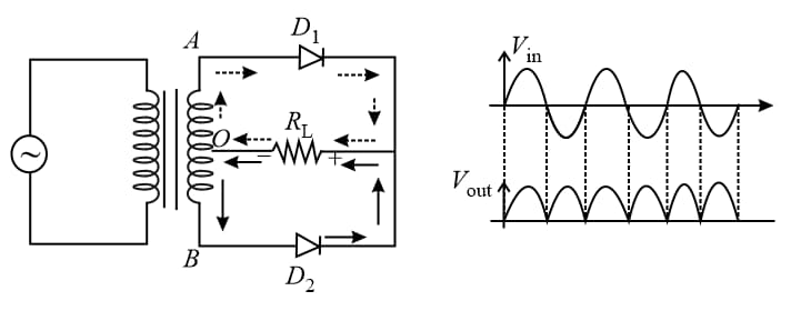
It rectifies both halves of input signal.
(i) Average output:
(ii) RMS output:
(iii) Ripple factor:
(iv) Ripple frequency: This ripple frequency of full-wave rectifier (frequency of input )
(v) Peak inverse voltage : It’s value is .
(vi) Efficiency: for
11. Transistor:
Junction transistors are of two types:
(i) transistor: It is formed by sandwiching a thin layer of -type semiconductor between two - type semiconductors.
(ii) transistor: It is formed by sandwiching a thin layer of -type semiconductor between two - type semiconductors.
Different modes of operation of a transistor:
| Operating mode | Emitter base bias | Collector base bias |
| Active | Forward | Reverse |
| Saturation | Forward | Forward |
| Cut off | Reverse | Reverse |
| Inverse | Rever | Forward |
Relation between currents in a transistor is and .
12. Transistor as CB amplifier:
(i) current gain: constant
(ii) current gain: . Value of lies between to
(iii) Voltage gain: Resistance gain
(iv) Power gain
13. Transistor as CE Amplifier:
(i) AC current gain: constant
(ii) DC current gain:
(iii) Voltage gain: Resistance gain
(iv) Power gain Resistance gain
Relation between and : or
14. Logic Gate and Truth Table:
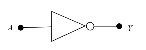
(i) NOT gate:
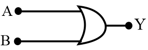
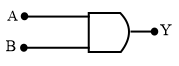
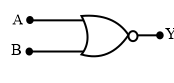
(ii) Truth tables for OR, AND, NOR and NAND gates:
| Input: A | Input: B |
OR gate
|
AND gate
|
NOR gate
|
NAND gate
|
| 0 | 0 | 0 | 0 | 1 | 1 |
| 0 | 1 | 1 | 0 | 0 | 1 |
| 1 | 0 | 1 | 0 | 0 | 1 |
| 1 | 1 | 1 | 1 | 0 | 0 |

15. Basic Boolean postulates and laws:
(i) Boolean Postulates: and
(ii) Identity law: , and
(iii) Negation law:
(iv) Commutative law: , and
(v) Associative law: , and
(vi) Distributive law: , and
(vii) Absorption laws:
(viii) Boolean identities: ,
(ix) De Morgan’s theorem: It states that the complement of the whole sum is equal to the product of individual complements and vice versa i.e. and .
16. Basic components of a communication system:
Faithful transmission of information from one place to another place is called communication.
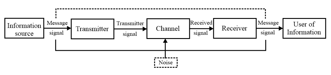
17. Transmitter:
A transmitter converts the message signal produced by the information source into a form (e.g. electrical signal) that is suitable for transmission through the channel to the receiver.
18. Communication channel:
A communication channel is a medium (transmission line, an optical fibre or free space etc) that connects a receiver and a transmitter. It carries the modulated wave from the transmitter to the receiver.
19. Receiver:
It receives and decodes the signal into its original form.
20. Important terms used in communication:
Transducer: A transducer is a device that converts one form of energy into another. For example microphone, photodetectors and piezoelectric sensors are types of the transducer.
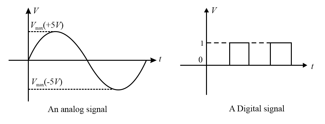
Signal: Signal is the information converted in electrical form. Signals can be analog or digital. Sound and picture signals in TV are analog.
It is defined as a single-valued function of time that has a unique value at every instant of time.
(i) Analog Signal: A continuously varying signal (Voltage or Current) is called an analog signal. A decimal number with a system base is used to deal with analog signals.
(ii) Digital Signal: A signal that can have only discrete stepwise values is called a digital signal. A binary number system with base is used to deal with digital signals.
(iii) Noise: There are unwanted signals that tend to disturb the transmission and processing of message signals. The source of noise can be inside or outside the system.
(iv) Attenuation: It is the loss of strength of a signal while propagating through a medium. It is like the damping of oscillations.
(v) Amplification: It is the process of increasing the amplitude (and therefore the strength) of a signal using an electronic circuit called the amplifier. Amplification is absolutely necessary to compensate for the attenuation of the signal in communication systems.
(vi) Range: It is the largest distance between the source and the destination upto which the signal is received with sufficient strength.
(vii) Repeater: A repeater acts as a receiver and a transmitter. A repeater picks up the signal which is coming from the transmitter, amplifies and retransmits it with a change in carrier frequency. Repeaters are necessary to extend the range of a communication system as shown in figure A communication satellite is basically a repeater station in space.

21. Bandwidth:
Bandwidth of signals: Different signals used in a communication system such as voice, music, picture, computer data etc. all have different ranges of frequency. The difference of maximum and minimum frequency in the range of each signal is called the bandwidth of that signal.
Bandwidth can be of message signal as well as of transmission medium.
(i) Bandwidth for analog signals: Bandwidth for some analog signals are listed below:
| Signal | Frequency Range | Bandwidth Required |
| Speech | ||
| Music | High frequencies produced by musical instrument audible range | |
| Picture | - | |
| TV | Contains both voice and pictures |
(ii) Bandwidth for digital signal: Basically digital signals are rectangular waves and these can be splitted into a superposition of sinusoidal waves of frequencies where n is an integer extending to infinity. This implies that the infinite bandwidth is required to reproduce the rectangular waves. However, for practical purposes, higher harmonics are neglected for limiting the bandwidth.
22. Bandwidth of Transmission Medium:
Different types of transmission media offer different band width of which some are listed below,
| Service | Frequency Range | Remarks | |
| 1 |
Wire (most common: Coaxial Cable) |
Normally operated below | |
| 2 | Free space (radio waves) | ||
| (i) Standard AM | |||
| (ii) FM | |||
| (iii) Television | VHF (Very high frequencies) TV UHF (Ultra high frequency) TV | ||
| (iv) Cellular mobile radio | Mobile to Base Station and Base station to mobile | ||
| (v) Satellite Communication |
Unlinking Downlinking |
||
| 3 | Optical communication using fibers |
(microwaves-ultraviolet) |
One single optical fibre offers bandwidth |
23. Ground Wave Propagation:
(i) The radio waves which travel through the atmosphere following the surface of the earth are known as ground waves or surface waves and their propagation is called ground wave propagation or surface wave propagation. These waves are vertically polarized in order to prevent short-circuiting of the electric component. The electric field due to the wave-induced charges on the earth's surface. As the wave travels, the induced charges in the earth also travel along with it. This constitutes a current on the earth's surface. As the ground wave passes over the surface of the earth, it is weakened as a result of energy absorbed by the earth. Due to these losses, the ground waves are not suited for very long-range communication. Further, these losses are higher for high frequency. Hence, ground wave propagation can be sustained only at low frequencies .
(ii) The ground wave transmission becomes weaker with the increase in frequency because more absorption of ground waves takes place at a higher frequency during propagation through the atmosphere.
(iii) The ground wave propagation is suitable for low and medium frequency i.e. upto only.
(iv) The ground wave propagation is generally used for local band broadcasting and is commonly called a medium wave.
(v) The maximum range of ground or surface wave propagation depends on two factors:
(vi) The frequency of the radio waves and (ii) Power of the transmitter.
24. Sky Wave Propagation:
(i) The sky waves are the radio waves of frequency between to .
(ii) The ionospheric layer acts as a reflector for a certain range of frequencies ( to ). Therefore it is also called ionospheric propagation or short wave propagation. Electromagnetic waves of frequencies higher than penetrate the ionosphere and escape.
(iii) The highest frequency of radio waves which when sent straight (i.e. normally) towards the layer of ionosphere gets reflected from the ionosphere and returns to the earth is called critical frequency. It is given by is the number density of electron per .
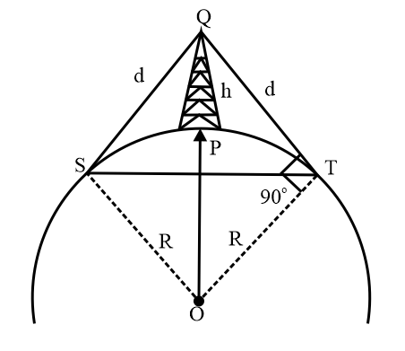
25. Space wave propagation:
(i) The space waves are the radio waves of very high frequency (i.e. between to or more.
(ii) The space waves can travel through the atmosphere from transmitter antenna to receiver antenna either directly or after reflection from the ground in the earth's troposphere region. That is why space wave propagation is also called tropospheric propagation or line of sight propagation.
(iii) The range of communication of space wave propagation can be increased by increasing the heights of transmitting and receiving antennas.
(iv) Height of transmitting Antenna:
The transmitted waves, travelling in a straight line, directly reach the received end and are then picked up by the receiving antenna as shown in the figure. Due to the finite curvature of the earth, such waves cannot be seen beyond the tangent points and .
As So
Area covered for TV transmission:
Population covered population densityarea covered.
If the height of the receiving antenna is also given in the question, then the maximum line of sight is,
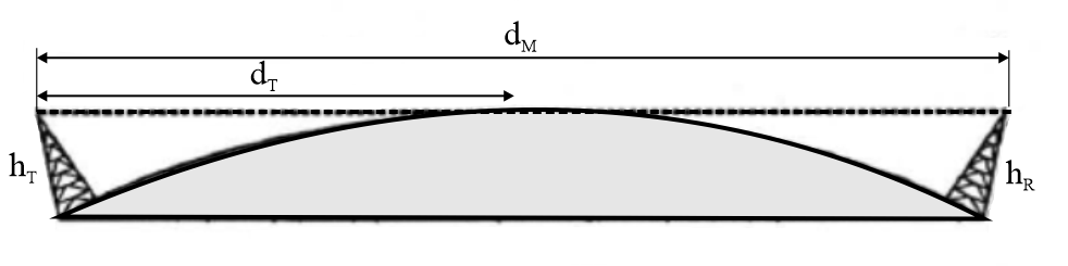
Where,
the radius of the earth (approximately )
height of transmitting antenna
height of receiving antenna
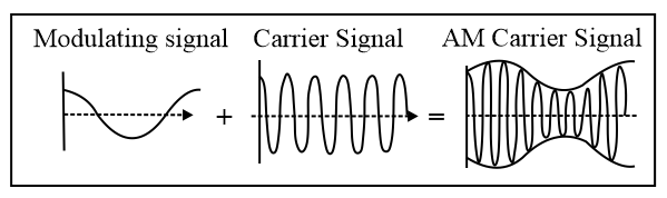
26. Modulation:
The phenomenon of superposition of information signal over a high-frequency carrier wave is called modulation. In this process, the amplitude, frequency or phase angle of a high-frequency carrier wave is modified in accordance with the instantaneous value of the low-frequency information.

27. Need for Modulation:
(i) To avoid interference: If many modulating signals travel directly through the same transmission channel, they will interfere with each other and result in distortion.
(ii) To design antennas of practical size: The minimum height of the antenna (not of the antenna tower) should be , where is the wavelength of modulating signals. This minimum size becomes impractical because the frequency of the modulating signal can be upto which corresponds to a wavelength of . This will require an antenna of the minimum height of . This size of an antenna is not practical.
(iii) Effective Power Radiated by an Antenna: A theoretical study of radiation from a linear antenna (length shows that the power radiated is proportional to (frequency)2 i.e. . For a good transmission, we need high powers and hence this also points out the need for using the high-frequency transmission.
Amplitude Modulation:
Modulation factor,
If and then
As the amplitude of the carrier wave varies at a signal frequency so the amplitude of wave & frequency of wave
Therefore
28. Frequency spectrum of AM wave:
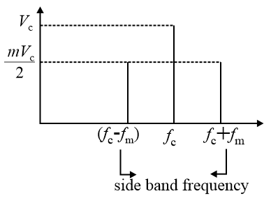
29. Power in AM wave:
Power of carrier wave where resistance of antenna in which power is dissipated.
Total power of sidebands:
Total power of AM wave
Fraction of total power carried by sidebands
30. Frequency Modulation (FM):
When the frequency of the carrying wave is changed in accordance with the instantaneous value of the modulating signal, it is called frequency modulation.

31. Modulation factor or index and carrier swing (CS)
(i) Modulation factor :
(ii) Carrier Suing (CS):
The total variation in frequency from the lowest to the highest is called the carrier swing
(iii) Side Bands:
FM wave consists of an infinite number of side frequency components on each side of the carrier frequency & soon.
| Amplitude Modulation | Frequency Modulation | ||
| 1 | The amplitude of wave is constant, whatever be the modulation index. | 1 | Modulation The amplitude of AM signal varies depending on the modulation index. |
| 2 | . It requires a much wider channel Bandwidth to times as compared to . | 2 | Bandwidth is very small (One of the biggest advantages). |
| 3 | Transmitters are complex and hence expensive. | 3 | Relatively simple and cheap. |
| 4 | Area of reception is small since it is embedded in the line of sight. This limits the FM mobile communication over a wide area) | 4 | The reception area is Large. |
| 5 | Noise can be easily minimized; amplitude variation can be eliminated by using a limiter. | 5 | It is difficult to eliminate the effect of noise. |
| 6 | Power contained in the wave is useful. Hence full transmitted power is useful. | 6 | Most of the power which is contained in carriers is not useful. Therefore, carrier power transmitted is a waste. |
| 7 | The average power is the same as the carrier wave. | 7 | The average power in a modulated wave is greater than carrier power. |
| 8 | No restriction is placed on the modulation index . | 8 | Maximum otherwise over modulation would result in distortion. |
| 9 | It is possible to operate several Independent transmitters on the same frequency. | 9 | It is not possible to operate without interference. |
32. Modem:
The name modem is a contraction of the terms Modulator and Demodulator. Modem is a device that can modulate as well as demodulate the signal.
33. FAX (Facsimile Telegraphy):
FAX is an abbreviation for facsimile which means exact reproduction. The electronic reproduction of a document at a distance place is called Fax.


