
EASY
JEE Main/Advance
IMPORTANT
Earn 100
The depletion region of junction has a thickness of the order of
50% studentsanswered this correctly
Important Questions on Semiconductor Electronics: Materials, Devices and Simple Circuits
MEDIUM
JEE Main/Advance
IMPORTANT
In a properly biased transistor
EASY
JEE Main/Advance
IMPORTANT
In an transistor, the collector current is . If of the electrons emitted reaches the collector, then the emitter current will be about
EASY
JEE Main/Advance
IMPORTANT
Application of a forward bias to a junction
MEDIUM
JEE Main/Advance
IMPORTANT
lntrinsic semiconductor at absolute zero temperature is a
MEDIUM
JEE Main/Advance
IMPORTANT
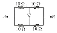
Four equal resistors, each of resistance , are connected as shown in the circuit diagram The equivalent resistance between and is
EASY
JEE Main/Advance
IMPORTANT
In a semiconducting material, the mobilities of electrons and holes are and , respectively. Which of the following is true?
MEDIUM
JEE Main/Advance
IMPORTANT
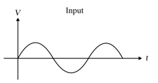
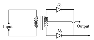
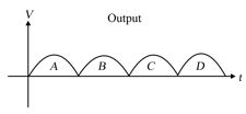
A full-wave rectifier circuit along with input and output are shown in the figure. The contribution from the diode is (are)
MEDIUM
JEE Main/Advance
IMPORTANT
In a junction having depletion layer of thickness , the potential difference across it is . The electric field is


