EASY
Earn 100

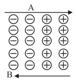
The diagram shows the formation process of a p-n junction diode Identify the arrow representing

(i) Electron Diffusion

(ii) Electron Drift

Question Image

Important Questions on Electronic Devices Semiconductors

MEDIUM
Which of the following statements is NOT TRUE for a semiconductor or a semiconductor device?
MEDIUM
The reading of the ammeter for a silicon diode in the given circuit is:

Question Image
EASY
What is 'depletion region' in a semiconductor diode?
EASY
The barrier potential of a p-n junction depends on:
a type of semi-conductor material
b amount of doping
c temperature
Which one of the following is correct?
EASY
In a p-n junction, an electric field of 5×10⁵ V m exists in the depletion region. The minimum kinetic energy of a conduction electron, in order to diffuse from n-side to the p-side, is found to be 3.2×10⁻²⁰ J. The width of the depletion region is,
EASY
In an unbiased p - n junction electrons diffuse from n-region to p-region because:
EASY
A potential barrier of 0.2 V exists across a PN juction.If the depletion region is 5×10⁻⁷ m wide. The intensity of electric field in this region is __________V/m
EASY
Explain the terms 'depletion layer' and 'potential barrier' in a p-n junction diode. How are the (a) width of depletion layer, and (b) value of potential barrier affected when the p-n junction is forward biased ?
EASY
How does an increase in doping concentration affect the width of depletion layer of a p-n junction diode?
MEDIUM
The contribution to the total current in a semiconductor, due to electrons and holes are 0.75 and 0.25 respectively. The drift velocity of electrons is 32 times that of holes at this temperature. Then the ratio between electron concentration and hole concentration is
EASY
The width of the depletion region in, p-n junction diode is 500 nm, and an electric field of 6×10⁵ V m-1 is also found to exist. The height of the potential barrier is
EASY
An intrinsic semiconductor is converted into n-type extrinsic semiconductor by doping it with:-
EASY

Given below are two statements: one is labelled as Assertion A and the other is labelled as Reason R

Assertion A: Diffusion current in a p-n junction is greater than the drift current in magnitude if the junction is forward biased.

Reason R: Diffusion current in a p-n junction is form the n-side to the p-side if the junction is forward biased.

In the light of the above statements, choose the most appropriate answer from the options given below.

EASY

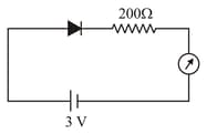
In the following circuit diagram, the current through the battery is

Question Image

MEDIUM
The density of an electron-hole pair in pure germanium is 3×10¹⁶ m-3 at room temperature. On doping with aluminium, the hole density increases to 4.5×10²² m-3. Now the electron density (in m-3 ) in doped germanium will be
MEDIUM

In a semiconductor diode, what is meant by a potential barrier?
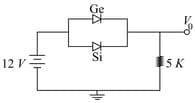
EASY
The depletion layer thickness of a p - n junction is 10-6 m. If the potential across it is 0.2 V, then the electric field will be
MEDIUM

Ge and Si diodes start conducting at 0.3 V and 0.7 V respectively. In the following figure if Ge diode connection are reversed, the value of V0 changes by: (assume that the Ge diode has large breakdown voltage)

Question Image