
P-N Junction Diode
P-N Junction Diode: Overview
This topic covers concepts, such as p-n Junction, Potential Barrier at the Junction Diode, Depletion Region at the Junction Diode, Forward Biasing of Junction Diode, Reverse Biasing of Junction Diode, Characteristic Curve of Junction Diode, etc.
Important Questions on P-N Junction Diode
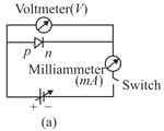
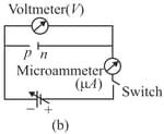
Which of the following circuit diagram of p – n junction diode is (i) forward bias and in (ii) reverse bias:
Which of the following statements is NOT TRUE for a semiconductor or a semiconductor device?
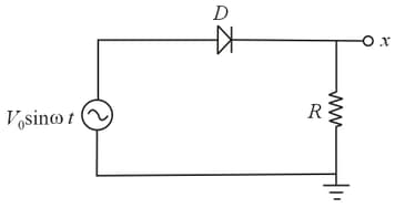
An ideal diode and a resistance are connected in series with an alternating voltage source . If the root-mean-square value of the voltage is measured at the point , as shown, the result will be
The breakdown that occurs in reverse bias conditions in a narrow junction diode is known as
Reverse saturation current of a diode:
Pick out the incorrect statement regarding reverse saturation current in the p-n junction diode.
The electric field in the depletion layer of an unbiased p-n junction is;
When the p-n junction diode is reverse biased, the thickness of the depletion layer;
When a p-n junction diode is reverse biased;
The main cause of zener breakdown is
Reverse bias applied to a junction diode.
Beyond the threshold voltage, resistance offered by the diode is:
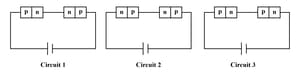
Two identical PN junction are joined in series with a battery shown below. For which potential drop is same.
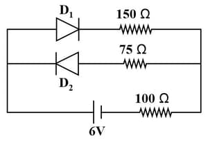
The circuit shown below contains two ideal diodes, each with a forward resistance of If the battery voltage is the current through the resistance (in amperes) is:
In reverse bias of a p-n junction diode, the reverse current is very small and is voltage independent upto certain reverse bias voltage, known as
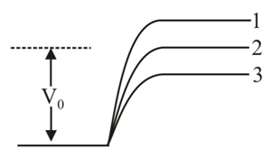
In figure, is the potential barrier across a junction, when no battery is connected across the junction.
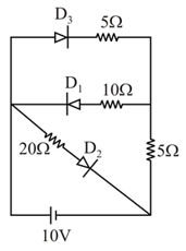
In the given circuit, Current through the battery is :-
The mobility of free electron is greater than holes because :-


