p-n Junction Diode
p-n Junction Diode: Overview
This topic covers concepts such as p-n Junction, Potential Barrier at the Junction Diode, Depletion Region at the Junction Diode, Forward Biasing of Junction Diode, Reverse Biasing of Junction Diode, and Characteristic Curve of Junction Diode.
Important Questions on p-n Junction Diode
Which of the following circuit diagram of p – n junction diode is (i) forward bias and in (ii) reverse bias:
The breakdown mechanism in a lightly doped P-N junction under reverse biased condition is called _____ breakdown.
Low doping required for Avalanche breakdown in diodes.
The breakdown that occurs in reverse bias conditions in a narrow junction diode is known as
Reverse saturation current of a diode:
Pick out the incorrect statement regarding reverse saturation current in the p-n junction diode.
The electric field in the depletion layer of an unbiased p-n junction is;
When the p-n junction diode is reverse biased, the thickness of the depletion layer;
When a p-n junction diode is reverse biased;
The main cause of zener breakdown is
Reverse bias applied to a junction diode.
For a p-n junction normal diode and a Zener diode, which of the following statements is true?
The reading of the ammeter for a silicon diode in the given circuit is:

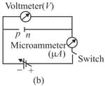
Currents flowing in each of the following circuits and respectively are
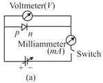
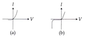
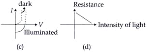
Identify the semiconductor devices whose characteristics are given below, in the order :
The forward-biased diode connection among the following is:
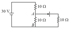
Find for the circuit given below.
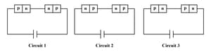
Two identical PN junction are joined in series with a battery shown below. For which potential drop is same.
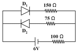
The circuit shown below contains two ideal diodes, each with a forward resistance of If the battery voltage is the current through the resistance (in amperes) is: