
Extrinsic Semiconductor
Extrinsic Semiconductor: Overview
This topic consists of various concepts like Extrinsic Semiconductor,Doping and Dopant,Doping, etc.
Important Questions on Extrinsic Semiconductor
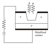
The diagram below is showing:
An intrinsic semiconductor has atoms and carrier concentration . If it is doped by a pentavalent impurity in the ratio , then calculate the number density of holes as charge carriers.
An intrinsic semiconductor has atoms and the carrier concentration . If it is doped by a pentavalent impurity in the ratio , then calculate number density of holes as charge carriers.
In a -type semiconductor, which of the following statement is true?
An N-type silicon sample of width thickness and length carries a current of when the voltage is applied across the length of the sample. What is the current density? If the free electron density is , then find how much time it takes for the electrons to travel the full length of the sample.
For a pure Si crystal has atom $\mathrm{m}^{-3}$. It is doped by PPM concentration of pentavalent As. Calculate the number of electron & holes.
(Given that )
In a pure semiconductor crystal of , if antimony is added then what type of extrinsic semiconductor is obtained. Draw the energy band diagram of this extrinsic semiconductor so formed.
Explain the process of doping.
When an intrinsic semiconductor such as is doped with a small amount of a trivalent impurity like boron
The intrinsic carrier concentration in silicon at is known to be . A sample of silicon is doped with arsenic (a group element). Under these circumstances the concentrations of electrons and holes in the sample are
Intrinsic carrier concentration of a silicon sample at is After doping, the number of majority carriers is The minority carrier density is
The base region of a silicon n-p-n transistor is obtained by doping with either
What are minority current carriers in Extrinsic semiconductor.
Which of the following energy band diagram shows the N-type semiconductor
In -type semiconductor, Silicon is doped with
What is type of majority charge carriers present in p-type semiconductor?
No crystal is found to be prefect at room temperature. The defects present in the crystals can be stoichiometric or non-stoichiometric. Due to nonstoichiometric defects, the formula of the ionic compound is different from the ideal formula. For example, the ideal formula of ferrous oxide should be but actually in one sample, it was found to be . This is because the crystal may have some ferric ions in place of ferrous ions. These defects change the properties of the crystals. In some cases, defects are introduced to have crystals of desired properties as required in the field of electronics. Doping of elements of Group 14 with those of Group 13 or 15 is most common. In ionic compounds, usually impurities are introduced in which the cation has higher valency than the cation of the parent crystal, e.g., into .
Which one of the following doping will produce p-type semiconductor ?
The hole density and electron density in -type semiconductors are related as
Range of energy required by electron of valance band to move into hole is . The accepter energy level lies
Which of the following energy band diagram shows the N-type semiconductor


