p-n Junction and Semiconductor Diode
p-n Junction and Semiconductor Diode: Overview
This topic consists of various concepts like p-n Junction,Type of Junction Diode,Diffusion Current in Semiconductors, etc.
Important Questions on p-n Junction and Semiconductor Diode
Which of the following circuit diagram of p – n junction diode is (i) forward bias and in (ii) reverse bias:
If each diode has a forward bias resistance of in the below circuit,
Which of the following options is correct?
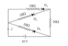
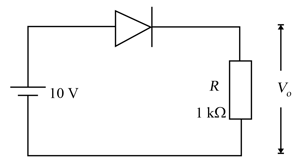
In the given circuit, the current through the battery will be
Given below are two statements: one is labelled as Assertion A and the other is labelled as Reason R
Assertion A: Diffusion current in a junction is greater than the drift current in magnitude if the junction is forward biased.
Reason R: Diffusion current in a junction is form the -side to the -side if the junction is forward biased.
In the light of the above statements, choose the most appropriate answer from the options given below.
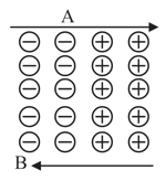
The diagram shows the formation process of a p-n junction diode Identify the arrow representing
(i) Electron Diffusion
(ii) Electron Drift
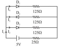
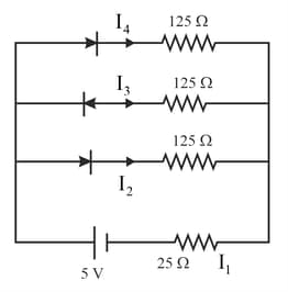
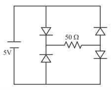
Following circuit contains diodes with forward bias having resistance and reverse bias having infinite resistance. The ratio of is equal to
In the given figure, a p-n Junction is
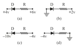
Categories each of the following junction diodes as either forward biased or reverse biased. Give reason for each answer.
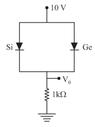
In an ON state, the individual Silicon and Germanium diodes, allow a voltage drop of and respectively across them. In the circuit shown, the Si and the Ge diode, are connected in a parallel combination to a voltage source of .
What is the voltage for the circuit network?
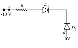
In the given circuit, the equivalent resistance (in ) betweenand is (if has positive
potential and has negative potential) (Diodes are assumed to be ideal)
ideal diodes are connected as shown in the circuit, the current through is
An ac voltage of peak value is connected in series with a silicon diode and a load resistor ( ). If the forward junction resistance of the diode is , then, peak diode current and peak load voltage are
Identify the incorrect statement with respect to depletion layer.
The increase in the width of the depletion region in a - junction diode is due to:
In diode, increasing the forward voltage, the thickness of depletion layer ____
Can a slab of p-type semiconductor be physically joined to another n-type semiconductor slab to form a p-n junction? justify your answer.
In the given circuit, the approximate value of voltage drop across is
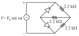
Sketch the voltage across the central resistor as a function of time. Take current in left direction as positive.
Is the drift current same as the diffusion current? are they in the same direction?
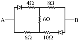
Find the current flowing between the points and in the following circuit. Take .